
Industries
Date: 2026-09-02
1、 Application scenarios
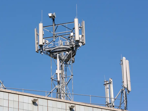
According to authoritative estimates, the usage of PCB by a single 5G base station is about 3.21 square meters, which is 1.76 times the usage of 4G base stations (1.825 square meters). At the same time, due to the higher frequency of 5G communication, there is a greater demand for PCB performance. Therefore, the unit price of PCB for 5G base stations is higher than that for 4G base stations. Overall, the value of PCB for a single base station in the 5G era is about three times that of the 4G era.
In addition, due to the higher spectrum of 5G, the coverage area of base stations is smaller. According to estimates, the number of 5G base stations in China will be 1.2-1.5 times that of 4G base stations, and more small base stations will also be needed. Therefore, the total number of base stations brought by 5G will be much more than that of 4G. It is expected that the new increment of 5G macro base stations in China during the peak of 5G construction in 2023 will be 1.5 times that of the peak of 4G construction in 2015. Based on comprehensive calculations, we believe that the market size of the communication PCB industry for base stations in the next few years will be about 2-4.5 billion US dollars. Compared to the 9-1.5 billion market in the 4G era, the PCB industry for base stations has undoubtedly experienced explosive growth in recent years.
The applications of communication PCBs mainly include wireless networks (communication base stations), transmission networks, data communication, and fixed broadband networks. There is a lack of data on applications other than wireless networks in the market. Therefore, this report mainly starts with the use of PCBs for wireless networks, that is, base stations, and analyzes the development prospects of the communication PCB industry in the next few years through point coverage. In the other three applications, except for fixed line broadband which has entered a mature stage with average growth rate in the future, the demand for PCBs in the transmission network industry will also increase with the construction of 5G. PCBs for data communication mainly rely on the completion of 5G network construction. As a promising application in the 5G industry (5G generates massive data, and the demand for data centers increases significantly), the future industry demand for PCBs should not be underestimated.
In the field of communication, PCBs are widely used in wireless networks, transmission networks, data communication, and fixed broadband networks. Related products include conventional high multilayer boards, high-speed multilayer boards, backboards, high-frequency microwave boards, soft hard composite boards, multifunctional metal substrates, etc.


|
Application Areas |
main equipment |
Related PCB products |
characteristics |
|
wireless network |
Communication base station |
Backboard, conventional multilayer board, high-speed multilayer board, high-frequency microwave board, multifunctional metal substrate |
Metal based, large-sized, high multilayer, high-frequency materials, and mixed pressure |
|
transmission network |
OTN transmission equipment, microwave transmission equipment |
Backboard, conventional multi-layer board, high-speed multi-layer board, high-frequency microwave board, soft hard bonding board |
High speed materials, large size, multiple layers, high density, multiple back drills, soft hard combination, high-frequency materials, and mixed pressure |
|
data communication |
Routers, switches, service/storage devices |
Backboard, conventional multi-layer board, high-speed multi-layer board, soft hard bonding board |
High speed materials, large size, high multiple layers, multiple back drills, soft hard combination |
|
Fixed broadband |
OLT, ONU and other fiber to the home devices |
Backboard, conventional multi-layer board, high-speed multi-layer board, soft hard bonding board |
Multilayer board, combination of soft and hard materials |
The communication and electronics industry accounts for approximately 5% -10% of our company's market share, making it a relatively large business area for our company. Our PCB is mainly used in communication electronics, including communication base stations, switches, routers, antennas, fiber optic interfaces, optical modules, storage devices, private network walkie talkies, etc.
2、 Difficulties in control
The production and manufacturing difficulty of PCB boards for communication electronics is much greater than that of circuit boards in other fields. Mainly due to the significant differences in form, large (or possibly small) size, high thickness, multiple special processes, strict signal control, and high dependence on special materials of communication PCB products. Specifically for the production and manufacturing of circuit boards, the following controls need to be implemented:
1. Different types of material processing capabilities
The first challenge in processing communication PCBs is to have the ability to process different types of boards. As mentioned earlier, due to the significant differences in the form of communication products, the demand for sheet metal is also diverse. Processing of different TG values from the most common FR4 sheet metal; Processing of materials from various brands such as ISOL's FR408, Panasonic's M4, M6, etc. for high-speed boards; Moving on to high-frequency sheet metal processing, such as processing PTFE sheets from various brands such as SYE-LNB33, S7136H, Rogers, TACONIC, ARLON, etc; Even: processing of pure copper based, iron-based, and ceramic based sheet metal. There are significant differences in the processing methods and key control points among them, which require long-term exploration to grasp the specific differences.
2. Production of precision circuits
Another key capability for producing communication PCBs is the ability to produce fine circuits. Due to the fact that communication circuit boards usually have requirements for impedance, DK, DF values, and frequency. The processing capability of the circuit is directly related to the product's ability. There may even be situations where the entire batch of finished products is scrapped due to the large etching tolerance of the circuit. This is a significant challenge for the control of circuit board factories.
3. Electroplating ability and hole filling ability
This is a crucial capability for producing such circuits. Firstly, the uniformity of electroplating directly affects the etching tolerance of the circuit, thereby affecting the performance of such PCBs. Secondly, due to the high number of layers in many communication circuit boards, the aspect ratio is very large, and having high aspect ratio electroplating capability is particularly important for the production of circuit boards. Thirdly, due to the fact that many communication PCBs have mechanical blind buried holes and HDI structures, having good resin hole filling ability and VCP hole filling ability is particularly important for the production of such PCBs.
4. Drilling ability
Communication circuit boards have extremely high requirements for drilling capabilities, which are reflected in the following two reasons: firstly, due to the special nature of the material, TPFE material is relatively brittle and causes significant wear on the drill bit. Therefore, it is necessary to use drill bits made of better materials as much as possible, and to control the lifespan, cutting speed, rotation speed, etc. of the drill bit; The second reason is that due to the thick thickness of the plate, some special drilling methods have to be used, such as back drilling, step-by-step drilling, cross drilling, etc.
5. Compression ability
The processing capability of compression is also a key factor affecting the success or failure of communication circuit boards. The most critical factor is the control of layer bias. Due to the high number of layers in communication, the occurrence of layer bias basically means that it will cause a short circuit and be scrapped. Another issue is due to the special nature of communication board materials. For example, many high-speed boards have TG values exceeding 200 ℃, while many high-frequency boards have TG values exceeding 280 ℃, which requires very high performance from the press.
How is the company managed and controlled?
In terms of materials, we have established certain connections with numerous high-frequency and high-frequency sheet metal suppliers to meet customers' needs for different brands of sheet metal. We have many years of PCB production experience and a deep understanding of the production characteristics of different types of board materials.
In terms of manufacturing: first-class equipment, making communication field circuit board equipment is the most basic guarantee. Our company has advanced LDI exposure machines, reliable circuit etching machines, electroplating with positive and negative film production capabilities, and deep control drilling machines and gong machines. Etching ability: The minimum line width/line width can reach 2mil, and the minimum tolerance can be ± 20% or 1.5mil; Electroplating ability: Our conventional aspect ratio can reach 12:1, and the ultimate aspect ratio can reach 20:1 (outsourced electroplating, with stable suppliers); Drilling: We have detailed control methods for drilling different substrates; For various special drilling methods, there is a mature control system. Compression: Our compression equipment is very powerful, with advanced CCD hot melt machines (deviation<2mil), fully automatic copper foil cutting and arranging machines, fully automatic reflow lines, and fully automatic laminating machines (maximum temperature of 300 ℃, temperature difference<2 ℃). In addition, we have multiple experienced process engineers who are familiar with the detailed control of communication and electronic PCBs.


3、 What communication and server clients do we have?
Our company has been in the field of communication electronics since 2010 and has a history of 11 years. With excellent product capabilities, we have received unanimous praise from our customers. Our clients in the field of communication electronics include:


4、 Future improvement direction
Communication electronics is not only the infrastructure of modern society, but also plays a crucial role in various fields such as economy, society, and national security, and its importance will continue to increase in the future. With the continuous breakthroughs of new technologies such as AI, new requirements have been put forward for the production and manufacturing of circuit boards. Therefore, our technical plan in the fields of communication electronics and servers is:
|
field |
project |
Process capability (now) |
Process capability (future) |
|
Communication and servers |
number of layers |
Sample 36 layers, batch 26 layers |
48 layers of samples, 36 layers for mass production |
| Line width/line spacing | ≥3mil/3mil | ≥2mil/2mil | |
| aspect ratio | Sample 20:1 layer, batch 12:1 layer | Sample 40:1 layer, batch 20:1 layer | |
| HDI order | 2nd order HDI | 3rd order HDI, arbitrary order HDI | |
| drilling | Normal drilling, back drilling, step-by-step drilling, opposite drilling | Improve the yield of special drilling methods | |
| Mixing ability | FR4 PTFE | PTFE ceramics, PTFE FR4 ceramics, PTFE fiberglass and other structures mixed pressure | |
| Processing capability of different materials | At present, the types that can be processed include FR4, high-speed plate, and high-frequency PTFE plate | Improve yield and enhance the performance of this type of product |



 Follow Us
 +86 13088807439
  E-mail